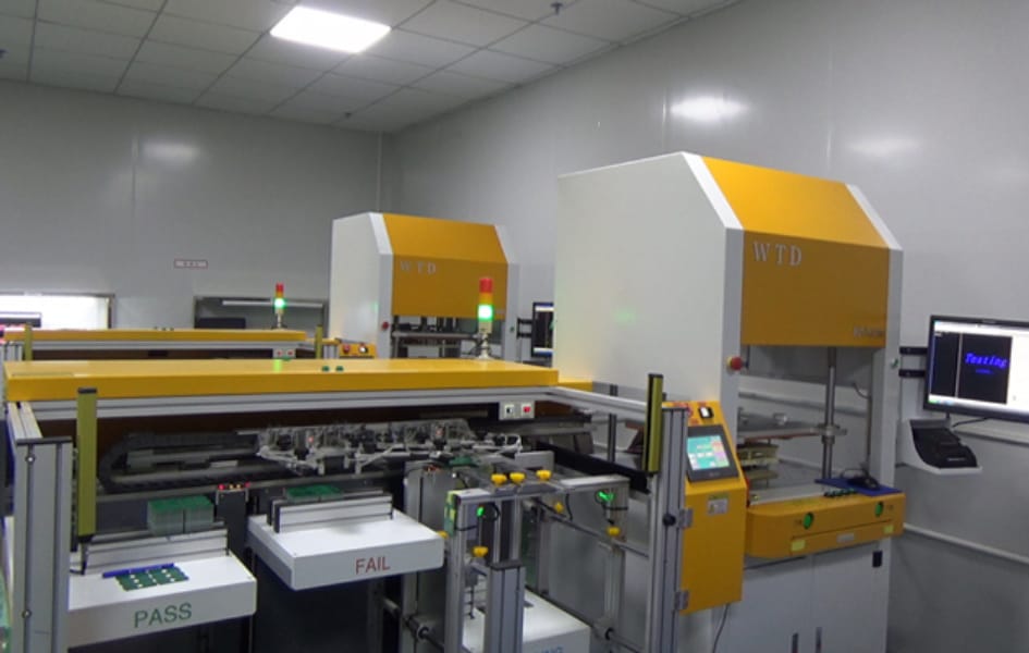
Manufacturing a PCB is a complex process that involves several steps. One of the key steps in making a PCB involves assembling the different components onto the board. This process is known as PCB assembly, and it involves using a method called PCB panelization.
So, what exactly is PCB panelization? Essentially, it is a process that involves arranging multiple PCBs onto a single panel. This is done to increase the production efficiency and reduce costs. By assembling multiple PCBs onto a single panel, the manufacturer can optimize the use of materials and minimize waste.
There are different ways to panelize a PCB, but the most common method used is called the “Step and Repeat” process. In this process, the same PCB design is repeated multiple times on a single panel, with a small gap between each copy. This gap is known as the “routing channel,” and it allows the individual boards to be separated from each other during the final stage of production.
The Step and Repeat process is usually done using specialized software that can generate a panel layout based on the given PCB design. Once the panel is designed, the PCB assembly process can begin. This involves placing the different components onto the individual boards, soldering them in place, and then removing the individual boards from the panel.
The PCB panelization process is critical to ensuring the efficient and cost-effective production of electronic devices. By arranging multiple PCBs onto a single panel, the manufacturer can optimize the production process and reduce costs. Additionally, panelization helps ensure that the final product meets the desired specifications and standards.
In summary, PCB panelization is the process of assembling multiple PCBs onto a single panel. This is done to increase production efficiency and reduce costs. The Step and Repeat process is the most common method used in panelization and involves repeating the same PCB design multiple times on a single panel. Overall, panelization is a critical step in the PCB assembly process and plays a crucial role in the production of electronic devices.