首先,從結構上看,PCB單板是由一塊完整的電路板組成的,其中包含了所有必要的電路連接和元器件安裝點。而拼板由多塊電路板通過接插件等方式連接在一起,彼此之間可以實現信號的傳輸和共享。因此,拼板的結構更加復雜,需要額外的連接線路。
其次,從用途上來說,PCB單板通常被用于相對簡單的電子設備中,如家用電器、手機等。因為它的結構簡單,易于制造和維修。而拼板則更多地應用于復雜的電子設備,如計算機、通信設備等。拼板的結構可以通過組合不同的電路板實現更復雜的功能,滿足更高的性能要求。
再次,從性能角度來看,PCB單板通常具有較低的成本和較短的制造周期。因此,對于需要快速上市的產品來說,PCB單板是一個較好的選擇。而拼板則通常具有更高的成本和制造周期,但可以提供更強大的性能和更高的擴展性。
綜上所述,PCB單板和拼板在結構、用途和性能等方面存在明顯的差異。根據實際需求,選擇適合的電路板類型可以更好地滿足產品的要求。
]]>
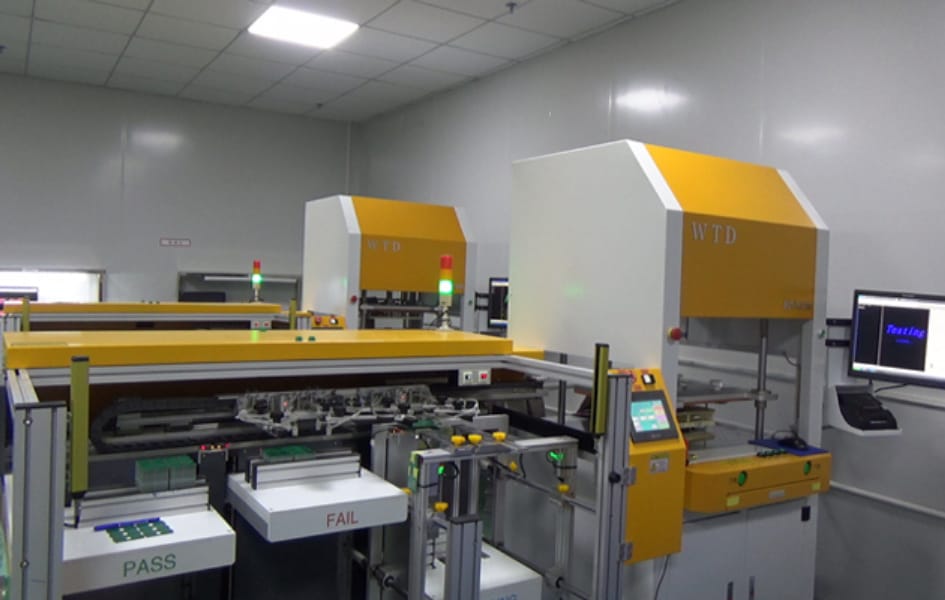
Manufacturing a PCB is a complex process that involves several steps. One of the key steps in making a PCB involves assembling the different components onto the board. This process is known as PCB assembly, and it involves using a method called PCB panelization.
So, what exactly is PCB panelization? Essentially, it is a process that involves arranging multiple PCBs onto a single panel. This is done to increase the production efficiency and reduce costs. By assembling multiple PCBs onto a single panel, the manufacturer can optimize the use of materials and minimize waste.
There are different ways to panelize a PCB, but the most common method used is called the “Step and Repeat” process. In this process, the same PCB design is repeated multiple times on a single panel, with a small gap between each copy. This gap is known as the “routing channel,” and it allows the individual boards to be separated from each other during the final stage of production.
The Step and Repeat process is usually done using specialized software that can generate a panel layout based on the given PCB design. Once the panel is designed, the PCB assembly process can begin. This involves placing the different components onto the individual boards, soldering them in place, and then removing the individual boards from the panel.
The PCB panelization process is critical to ensuring the efficient and cost-effective production of electronic devices. By arranging multiple PCBs onto a single panel, the manufacturer can optimize the production process and reduce costs. Additionally, panelization helps ensure that the final product meets the desired specifications and standards.
In summary, PCB panelization is the process of assembling multiple PCBs onto a single panel. This is done to increase production efficiency and reduce costs. The Step and Repeat process is the most common method used in panelization and involves repeating the same PCB design multiple times on a single panel. Overall, panelization is a critical step in the PCB assembly process and plays a crucial role in the production of electronic devices.