Manufacturing a PCB is a complex process that involves several steps. One of the key steps in making a PCB involves assembling the different components onto the board. This process is known as PCB assembly, and it involves using a method called PCB panelization.
So, what exactly is PCB panelization? Essentially, it is a process that involves arranging multiple PCBs onto a single panel. This is done to increase the production efficiency and reduce costs. By assembling multiple PCBs onto a single panel, the manufacturer can optimize the use of materials and minimize waste.
There are different ways to panelize a PCB, but the most common method used is called the “Step and Repeat” process. In this process, the same PCB design is repeated multiple times on a single panel, with a small gap between each copy. This gap is known as the “routing channel,” and it allows the individual boards to be separated from each other during the final stage of production.
The Step and Repeat process is usually done using specialized software that can generate a panel layout based on the given PCB design. Once the panel is designed, the PCB assembly process can begin. This involves placing the different components onto the individual boards, soldering them in place, and then removing the individual boards from the panel.
The PCB panelization process is critical to ensuring the efficient and cost-effective production of electronic devices. By arranging multiple PCBs onto a single panel, the manufacturer can optimize the production process and reduce costs. Additionally, panelization helps ensure that the final product meets the desired specifications and standards.
In summary, PCB panelization is the process of assembling multiple PCBs onto a single panel. This is done to increase production efficiency and reduce costs. The Step and Repeat process is the most common method used in panelization and involves repeating the same PCB design multiple times on a single panel. Overall, panelization is a critical step in the PCB assembly process and plays a crucial role in the production of electronic devices.
首先,我們需要判斷 PCB 打樣公司有沒有專業團隊。有專業團隊的公司能為客戶提供更好的解決方案,而且能夠更快速地解決客戶的問題。一個專業 PCB 打樣團隊需要具備電路設計、電子工程和 PCB 制作的技能和知識,能夠為客戶提供全方位的技術支持和合適的解決方案。
其次,我們需要留意 PCB 打樣公司的交貨時間。很多 PCB 打樣公司都能夠提供快速的交貨時間,但是這些時間是否可靠需要仔細考慮。在選擇 PCB 打樣公司時,我們應該選擇能夠提供穩定交貨時間的公司,確保客戶能夠按時收到他們所需的 PCB 產品。
接下來,我們需要考慮 PCB 打樣公司的制造能力。一個好的 PCB 打樣公司需要具備先進的設備和良好的生產設施。通過使用先進設備,公司能夠提供高品質的 PCB 制作服務,并能夠快速地生產大量的 PCB。
最后,我們需要考慮 PCB 打樣公司的信譽。選擇一個有良好信譽的 PCB 打樣公司非常重要,因為只有這樣能保證客戶的利益得到充分保障。尋找有良好信譽的 PCB 打樣公司可以在行業內咨詢,或者根據其他客戶的反饋來做出選擇。
關于這些方面,中國 PCBA 制造商深圳龍銘科技有限公司應該是一個非常好的選擇。深圳龍銘科技有限公司是一家專業的 PCB 打樣公司,具有長期的 PCB 制作經驗和良好的獲客反饋,其團隊成員都擁有多年的從業經驗,能夠為客戶提供專業的解決方案和技術支持。 此外,深圳龍銘科技有限公司還擁有先進的設備和齊全的生產設施,能夠保證 PCB 的制作質量,讓客戶放心購買。 相信在深圳龍銘科技的幫助下,客戶們一定能夠獲得滿意的 PCB 打樣服務。
在選擇 PCB 打樣公司時,您需要考慮多個因素。但無論您的選擇是什么,都應該確保選中的公司具有專業技能、穩定的交貨時間、良好的制造能力、以及良好的聲譽。深圳龍銘科技有限公司在這些方面均有優異表現,值得您考慮。
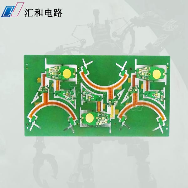
一、介紹匯和電路
匯和電路是一家專業從事 PCB 電路板制造的公司,總部位于深圳。公司成立于2003年,擁有自主研發的技術團隊和完整的質量管理體系,服務于全球范圍內的客戶。匯和電路致力于提供高品質、高效率、低成本的電路板制造服務,是業界優秀的 PCB 電路板供應商之一。
二、匯和電路的優勢
1. 專業的技術團隊
匯和電路的技術團隊由海內外電子行業的專業人士組成,具有豐富的 PCB 設計、制造和應用經驗。他們能夠對 PCB 制造過程中的各個環節進行嚴格控制和有效管理,確保產品的高品質和長期穩定性。此外,匯和電路還與多家頂尖研究機構進行技術合作,不斷推出創新的 PCB 電路板制造技術,為用戶提供更加優質的產品和服務。
2. 先進的生產設備
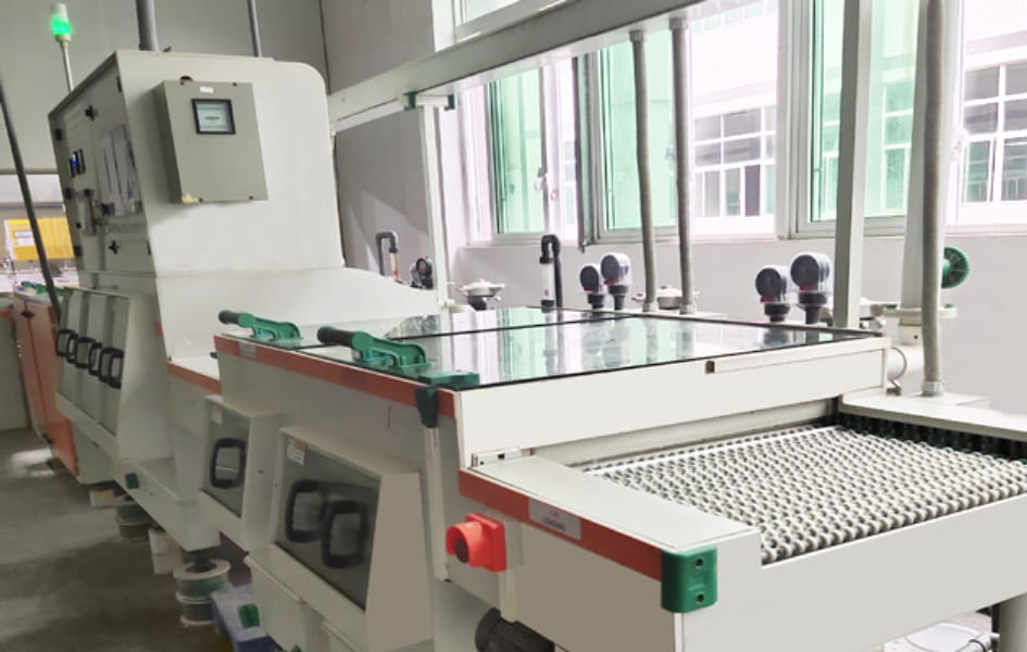
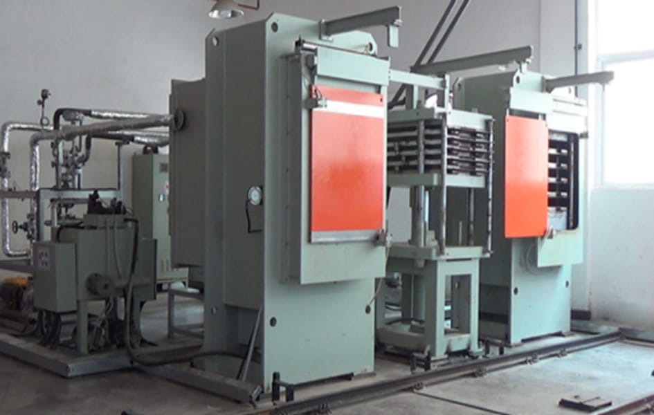
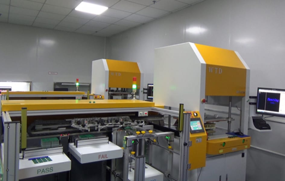
匯和電路擁有世界領先的 PCB 制造設備,包括高速車床、自動生產線、X光檢測儀等,能夠滿足不同級別、不同層數、不同復雜度的 PCB 電路板的生產需求。此外,匯和電路還通過了 ISO9001、UL認證及RoHS認證,產品符合各種國際標準,為用戶提供親和環保,高質量的產品和服務。
3. 優質的客戶服務
匯和電路為客戶提供全球化的客戶服務,包括即時在線咨詢,及時響應客戶需求,提供技術支持和解決實際問題等。為了提高客戶的滿意度,匯和電路不斷采取措施優化服務流程,降低成本,提高效率。
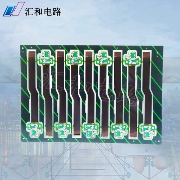
三、匯和電路的產品
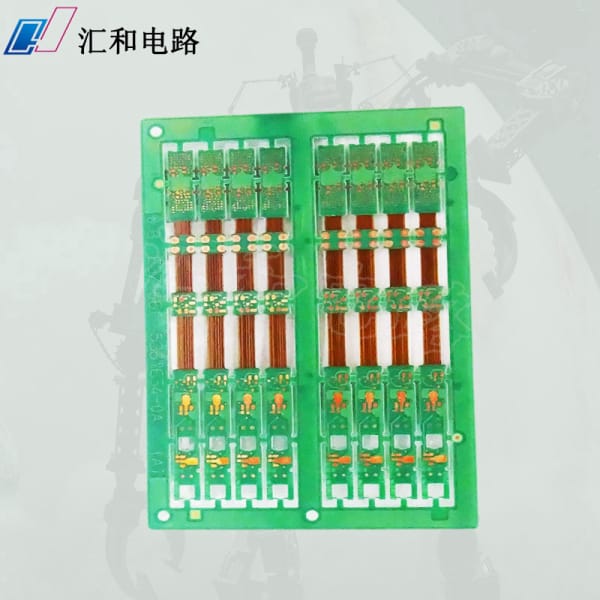
匯和電路的產品涵蓋了全球各種 PCB 電路板市場的需求,例如 FR4 PCB 板、Aluminum PCB 板、Flex PCB 板和MCPCB 等。匯和電路的產品有以下特點:
1. 高精度—— 世界領先的制造設備和嚴格的生產質量管控體系保證了高精度的 PCB 電路板;
2. 高可靠性—— 匯和電路堅持以“質量第一,信譽至上”的原則,認真負責地對 PCB 電路板進行檢測和檢驗,保證了產品的高可靠性;
3. 多樣性——除了標準 PCB 電路板產品外,匯和電路還能根據客戶需求,自定義板型和規格;
4. 快速交付——客戶下訂單后,匯和電路會盡最快速度制造出符合要求的 PCB 電路板,并按時交付。
]]>